Hybrid and Fusion Bonding Systems
Hybrid bonding extends fusion bonding with embedded metal pads in the bond interface, allowing face-to-face connection of wafers. The main application for hybrid bonding is advanced 3D device stacking.
Fusion or direct wafer bonding enables permanent connection via dielectric layers on each wafer surface used for engineered substrates or layer transfer applications such as backside illuminated CMOS image sensors.
Choose your Hybrid and Fusion Bonding System
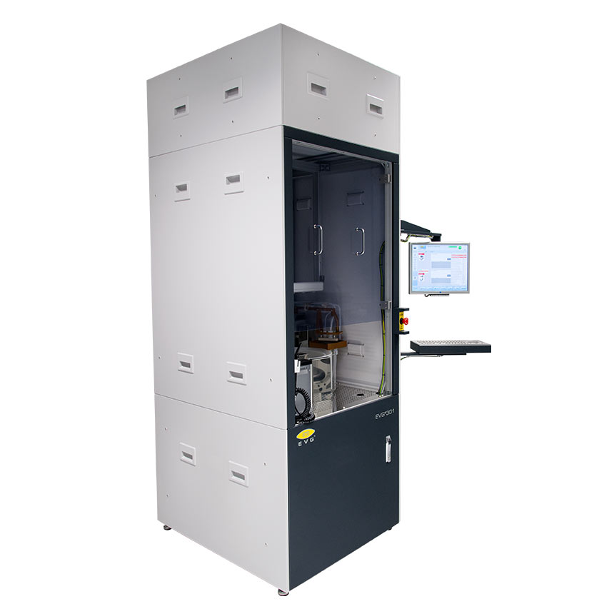
EVG®301
Single Wafer Cleaning System
R&D type single wafer cleaning system.
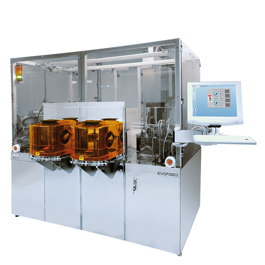
EVG®320
Automated Single Wafer Cleaning System
Automated single wafer cleaning system for efficient removal of particles.
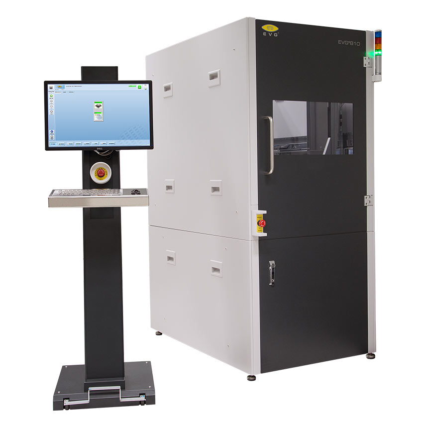
EVG®810 LT
Low Temp™ Plasma Activation System
Low-temperature plasma activation system for SOI, MEMS, compound semiconductors and advanced substrate bonding.
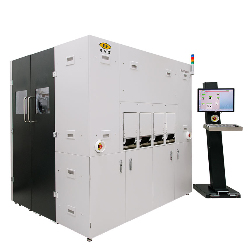
EVG®850 LT
Automated Production Bonding System for SOI and Direct Wafer Bonding
Automated production bonding system for a wide range of fusion/molecular wafer bonding applications.
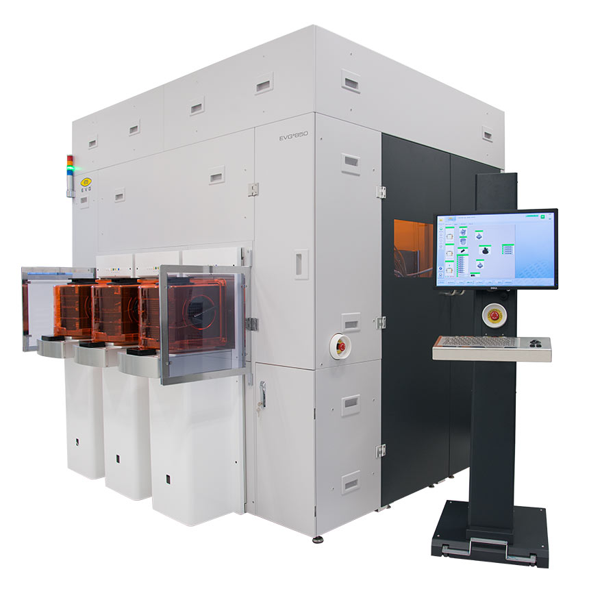
EVG®850
Automated Production Bonding System for SOI and Direct Wafer Bonding
Automated production bonding system for a wide range of fusion/molecular wafer bonding applications.
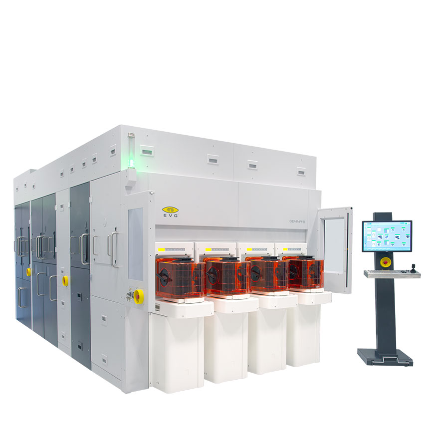
GEMINI® FB
Automated Production Wafer Bonding System
Integrated platform for high precision alignment and fusion bonding.
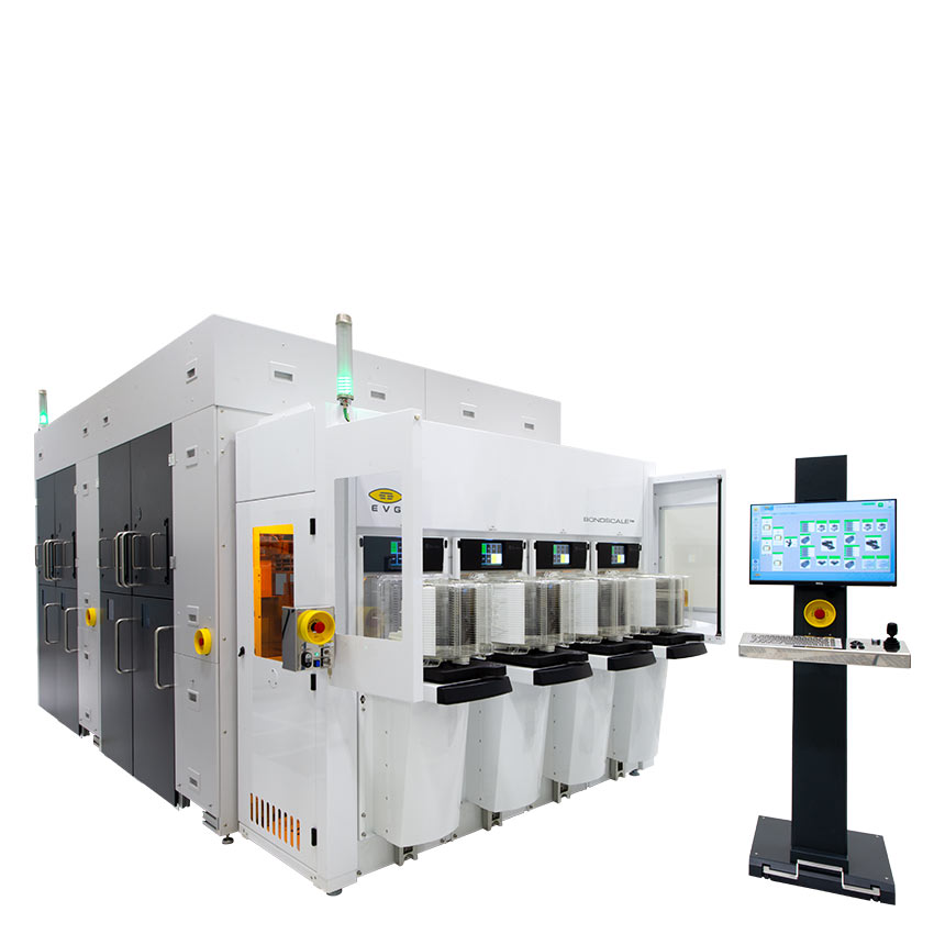
BONDSCALE®
Automated Production Fusion Bonding System
Enabling 3D Integration for More Moore.

Talk to our EVG product experts!
Questions?
Questions about our products and technologies?
Contact the EVG experts