- Products
-
Technologies
- IR LayerRelease™ Technology
- MLE™ - Maskless Exposure Technology
- Nanoimprint Lithography (NIL) - SmartNIL®
- Wafer Level Optics
- Optical Lithography
- Resist Processing Technology
- Temporary Bonding and Debonding
- Eutectic Bonding
- Transient Liquid Phase (TLP) Bonding
- Anodic Bonding
- Metal Diffusion Bonding
- Hybrid and Fusion Bonding
- Die-to-Wafer Fusion and Hybrid Bonding
- ComBond® Technology
- Metrology
- Company
- Careers
ComBond® High Vacuum Wafer Bonding Technology
A breakthrough technology driving the bonding of “anything on anything” enabling emerging and “beyond CMOS” device designs
Introduction
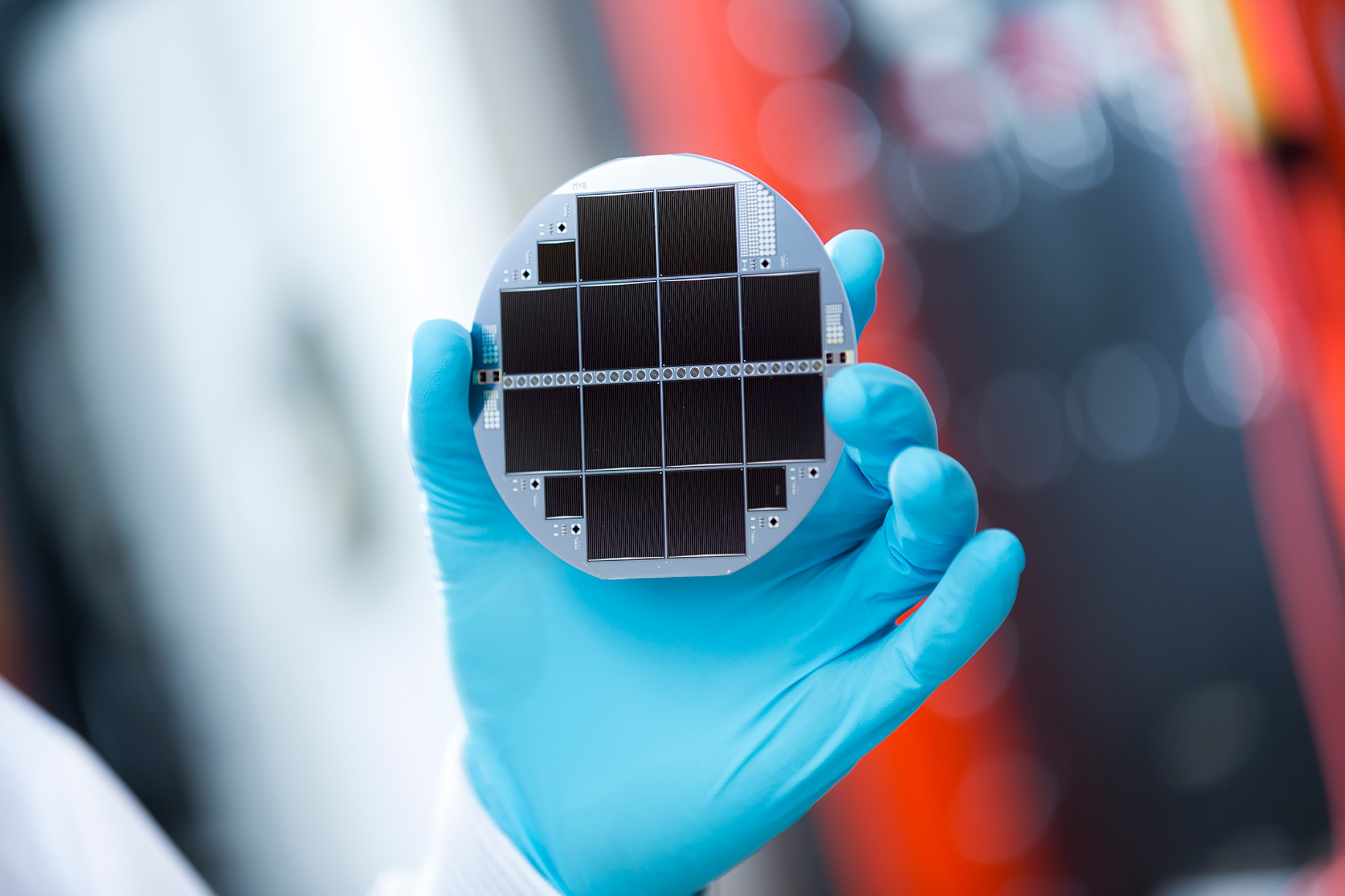
The ComBond technology adds a new milestone to EVG’s unique portfolio of wafer bonding equipment and technology in response to market needs for more sophisticated integration processes. The application areas range from advanced engineered substrates to high-end MEMS packaging, from “beyond CMOS” devices to stacked solar cells, and from high-performance logic to power devices.
The ComBond platform combines several technology breakthroughs to enable the formation of bond interfaces between heterogeneous materials at room temperature while achieving excellent bonding strength and electrical conductivity. Furthermore, ComBond enables the encapsulation of MEMS devices in high vacuum. Its capabilities include optical alignment with wafer clamping, programmable dehydration bake and getter activation, bonding in a bond chamber, and wafer handling done under high vacuum.
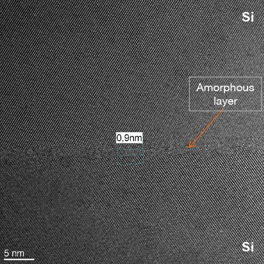
EVG’s breakthrough wafer activation technology and high-vacuum handling and processing allows the formation of covalent bonds at room or low temperature for the fabrication of engineered substrates and device structures. ComBond facilitates the bonding of heterogeneous materials with different lattice constant and coefficient of thermal expansion (CTE) as well as the formation of electrically conductive bond interfaces by its unique oxide-removal process. The ComBond high-vacuum technology also enables low-temperature bonding of metals, such as aluminum, that re-oxidize very fast in ambient environments. Void-free and particle-free bond interfaces and excellent bond strength can be achieved for all material combinations.
For vacuum encapsulation using aligned wafer bonding, the ComBond system advances its bonding capability through the addition of programmable dehydration bake and getter activation modules and the optical alignment module with wafer clamping. The high-vacuum handling and processing platform addresses rising demands for lower vacuum levels in leading-edge MEMS and other applications.
Market applications demanding room-temperature bonding of substrates with very different material properties include advanced engineered substrates, power devices, stacked solar cells and MEMS devices. The novel oxide-free bonding technique is particularly beneficial in silicon photonics, high-vacuum MEMS packaging, and compound semiconductor and other advanced engineered substrates for “beyond CMOS” applications such as high-mobility transistors, high-performance/low-power logic and radio frequency (RF) devices.
Features
- High-vacuum handling and processing (<7E-8 mbar) of wafers up to 200 mm
- Wafer surface activation
- Oxide-free direct bonding
- Room-temperature direct bonding
- Vacuum alignment capability
- Dehydration and bake-out of MEMS cavities
- High-vacuum encapsulation without getters
Related products

Talk to our EVG technology experts!
Questions?
Events

ICEP-HBS 2026
Listen to our talks:
“Hybrid Bonding and Interconnect Scaling: Driving Application Performance, Power and Cost by Mixing and Matching Semiconductor Technologies” by Representative Director Hiroshi Yamamoto.
“A predictive model for bond strengthening based on ion characteristics and the interface evolution in plasma activated fusion and hybrid bonding” by Deputy Team Leader Process Technology David Doppelbauer.
“From Scaling to Stacking: How Fusion and Hybrid Bonding enable Next-Generation High Performance Chip Architectures” by Business Development Manager Thomas Pleschke.
For more information click here.

Merck "The Future of Photonics — Materials Matter"
Listen to our talk “Enabling Scalable Photonic Packaging using Nanoimprint Lithography” held by Business Development Manager Andrea Kronawitter.
More information here.

CS / PIC / PE International Conference 2026
Visit us at our booth at the CS / PIC and PE International Conference and listen to our talks:
"High performance GaN power devices enabled by wafer bonding" held by Business Development Manager Elisabeth Brandl at the CS Conference.
"Advancing Photonic Packaging and Integration Through UV Nanoimprint Lithography" held by Senior Process Technology Engineer Patrick Schuster at the PIC Conference.
- IR LayerRelease™ Technology
- MLE™ - Maskless Exposure Technology
- Nanoimprint Lithography (NIL) - SmartNIL®
- Wafer Level Optics
- Optical Lithography
- Resist Processing Technology
- Temporary Bonding and Debonding
- Eutectic Bonding
- Transient Liquid Phase (TLP) Bonding
- Anodic Bonding
- Metal Diffusion Bonding
- Hybrid and Fusion Bonding
- Die-to-Wafer Fusion and Hybrid Bonding
- ComBond® Technology
- Metrology
Questions about our technologies?
Contact the EVG experts

