Anodic Bonding
Anodic bonding for interlayer free Si-glass bonding
Introduction
Anodic bonding is a technique to produce hermetic sealing between silicon/metals and glass insulators without using an intermediate layer. Borosilicate glass with high alkali ion concentration is a major requirement for this process. Different from other bonding techniques, anodic bonding involves heating and applying an electric field to the substrate materials.
Anodic bonding is also called field assisted bonding or electrostatic sealing. A clean wafer surface and atomic contact between the substrates is required for anodic bonding. Bonding takes place when the wafers are placed between the chuck and the temperature is increased to just below the glass transition temperature of glass, followed by applying electric potential of several hundred volts. After reaching a certain temperature, the oxides dissociate and alkali ions are driven into the glass by an electric field resulting in an oxygen-rich layer at the interface of the wafers. Oxygen ions are driven into the silicon surface by the electric field resulting in the formation of silicon dioxide. With specific applied pressure and voltage, the total bond process time is between 5 to 20 minutes.
Features
- Hermetic sealing
- Stable bonding
- Bonding below 4500C
- Low restrictions for Si surface
- High bond yield
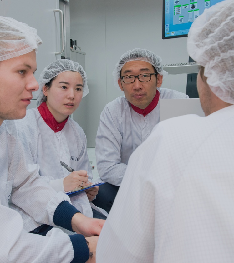
Talk to our EVG technology experts!
Questions?
Events
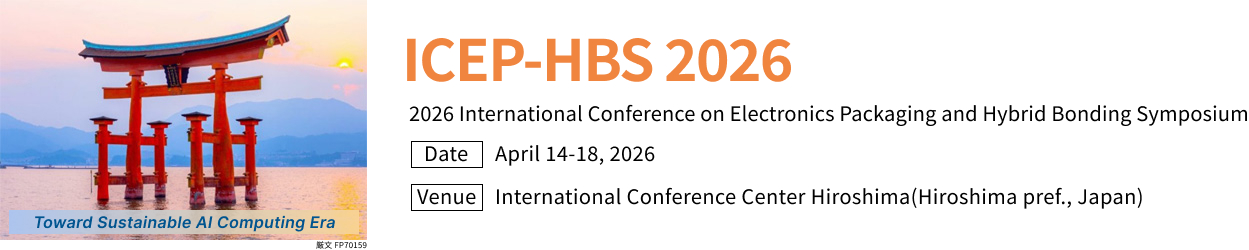
ICEP-HBS 2026
Listen to our talks:
“Hybrid Bonding and Interconnect Scaling: Driving Application Performance, Power and Cost by Mixing and Matching Semiconductor Technologies” by Representative Director Hiroshi Yamamoto.
“A predictive model for bond strengthening based on ion characteristics and the interface evolution in plasma activated fusion and hybrid bonding” by Deputy Team Leader Process Technology David Doppelbauer.
“From Scaling to Stacking: How Fusion and Hybrid Bonding enable Next-Generation High Performance Chip Architectures” by Business Development Manager Thomas Pleschke.
For more information click here.
Merck "The Future of Photonics — Materials Matter"
Listen to our talk “Enabling Scalable Photonic Packaging using Nanoimprint Lithography” held by Business Development Manager Andrea Kronawitter.
More information here.

CS / PIC / PE International Conference 2026
Visit us at our booth at the CS / PIC and PE International Conference and listen to our talks:
"High performance GaN power devices enabled by wafer bonding" held by Business Development Manager Elisabeth Brandl at the CS Conference.
"Advancing Photonic Packaging and Integration Through UV Nanoimprint Lithography" held by Senior Process Technology Engineer Patrick Schuster at the PIC Conference.
Questions about our technologies?
Contact the EVG experts