ZH
中文 (ZH)
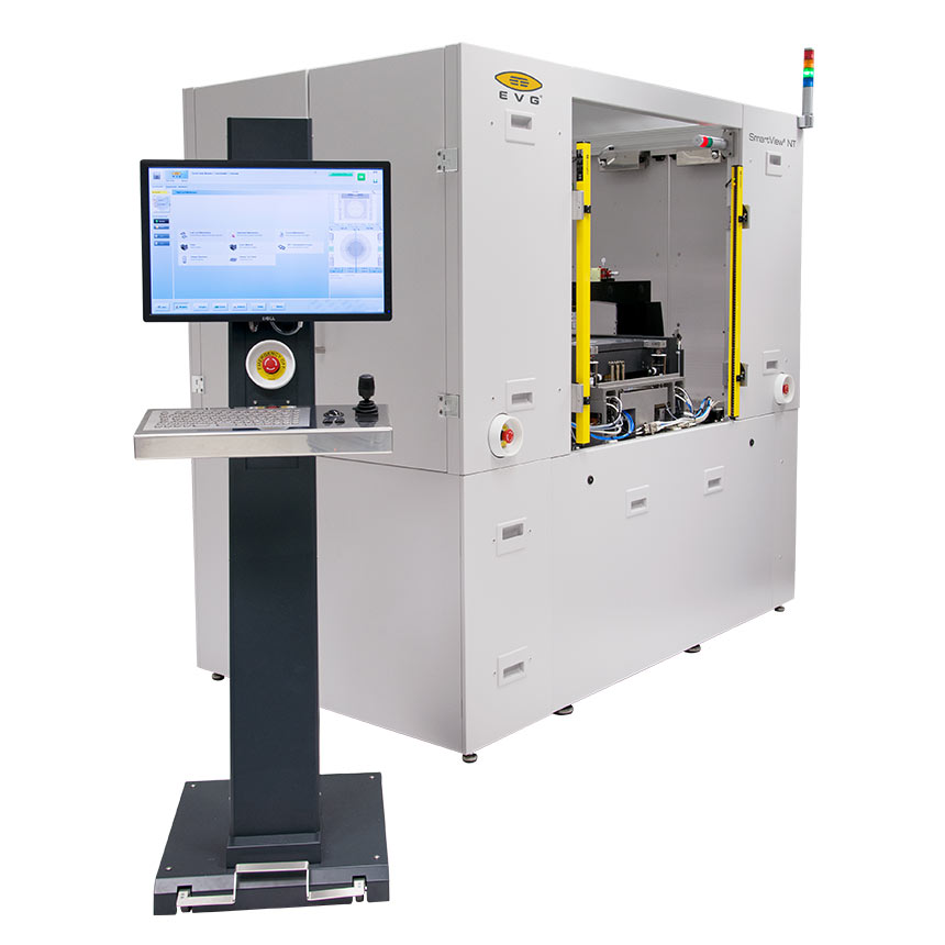
SmartView® NT
Automated Bond Alignment System for Universal Alignment
Fully automated bond alignment system for universal alignment with proprietary method for micron-level face-to-face wafer alignment
The SmartView NT automated bond alignment system for universal alignment offers a proprietary method for micron-level face-to-face wafer-level alignment. This alignment technique is key to achieving the required accuracy in multiple wafer stacks for leading-edge technologies. The tool is well suited for applications such as wafer stacking for 3D interconnects, wafer-level-packaging and high-volume MEMS devices.
Features
- Suitable for automated and integrated EVG bonding systems (EVG®560, GEMINI®) in 200 mm and 300 mm configurations
- Universal bond aligner (face-to-face-, backside-, infrared- and transparent alignment)
- No Z-axis motion and no refocusing required
- Windows® based user interface
- Bond pairs are aligned and clamped prior to loading into the bond chamber
- Manual or fully automated configurations (e.g. integration with GEMINI®)
- Options
- Can be combined with the EVG®500 series wafer bonding systems, EVG®300 series cleaning systems and EVG®810 LT plasma systems for a fully automated wafer-to-wafer alignment operation with cassette-to-cassette operation
Technical Data
| Substrate / Wafer parameters |
|---|
| Size: 150 - 200, 200 - 300 mm |
| Thickness: 0,1 - 5 mm |
| Max. stack height: 10 mm |
| Automatic alignment |
|---|
| Standard |
| Handling system |
|---|
| 3 cassette stations (up to 200 mm) or 2 FOUP load ports (300 mm) |

Talk to our EVG product experts!
Questions?
Questions about our products and technologies?
Contact the EVG experts
相关新闻
EV Group, Vietnam’s Authority of Information Technology Industry and PTIT Sign Memorandum of Understanding to Advance Vietnam's Semiconductor Capabilities
Mar, 2025
EV集团推出面向300毫米晶圆的下一代GEMINI®全自动生产晶圆键合系统,推动MEMS制造升级
Mar, 2025
EV Group Highlights Revolutionary Temporary Wafer Bonding and Debonding Solution for HBM and 3D DRAM at SEMICON Korea
Feb, 2025
