R&D Projects
Introduction
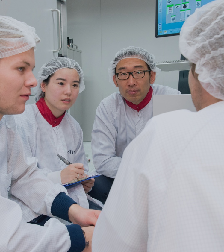
EVG is a leading supplier of equipment and process solutions for manufacturing semiconductors, MEMS, compound semiconductors, power devices, and nanotechnology devices.
The company actively participates in international R&D projects to expand its global reach and address the increasing demand for advanced sensor solutions.
Additionally, EVG engages in national research activities to enhance collaboration with local partners and support the development of a knowledge-based society by training the next generation of researchers in partnership with higher education institutions.
EVG positions itself as an ideal partner for research projects, whether in contract research or as a consortium partner in funded projects, contributing to the EU's objectives in various fields aiming to innovate and identify future technologies and trend.
Current Projects
TRANSFORM
TRANSFORM is an R&D project aiming to build a complete and competitive supply chain in EUROPE for PE based on SiC semiconductor technology. The consortium develop a complete and competitive PE value chain based on SiC semiconductors extending from wafers to inverters/converters, to be showcased in 5 applications.
The project aims to ensure the availability of machinery and equipment for the production of substrates and wafers up to the power electronics of European suppliers. This initiative is crucial for applications in automotive, industrial, renewable energy, and agricultural sectors.
The main objectives of the TRANSFORM project for silicon carbide (SiC) include advancing substrate technology to pilot line readiness, creating production equipment, and qualifying new substrates for industrial use. It also aims to develop enhanced planarMOS and trenchMOS technologies, optimize assembly and interconnect methods, and improve the design and architecture of SiC-based power electronic systems for better performance, reliability and cost-efficiency.
YESvGAN
The YESvGaN project is aiming to create a new class of vertical GaN power transistors that combine the high performance of vertical Wide Band Gap (WBG) transistors with the cost benefits of established silicon technology. These transistors are designed to replace IGBTs, reducing power conversion losses in various cost-sensitive applications, such as data center power supplies and electric vehicle traction inverters. The project encompasses the development of this new technology from wafer production to application. The YESvGaN consortium includes 23 industrial and research partners from 7 European countries.
The YESvGaN project aims to develop a new class of affordable and highly efficient Wide Band Gap (WBG) power transistors based on gallium nitride (GaN). These vertical GaN (vGaN) membrane transistors will be capable of handling voltages up to 1200 V and currents up to 100 A. The project will innovate across various parts of the semiconductor process chain, including low-cost substrates with thick epitaxy, vertical membrane approaches, and multiple transistor channel concepts.
ID2PPAC
ID2PPAC pursues the objective to demonstrate that Performance Power Area and Cost (PPAC) requirements for the 2nm node generation of leading-edge logic technology can be achieved. It consolidates and integrates 2nm technology solutions which have been identified and evaluated in its predecessor IT2.
The strength of the project pivots on the focused engagement of leading expert partners in these key interlocking areas and a shared pilot line.
The ID2PPAC project aims to enable IC-fabs to achieve EUV-based, single-print, high-volume manufacturing for the 2nm node by 2025. This advancement is driven by the increasing demand for compute power, which has led to a significant rise in interconnected devices—from 1 billion in the "PC era" to 10 billion in the "Mobile + cloud era," and an anticipated 100 billion in the future "Intelligence era." To support this growth, the semiconductor industry continues to innovate, following the trajectory predicted by Moore's Law, using lithography in combination with wafer bonding.
Related downloads
Talk to our EVG technology experts!
Questions?
Questions about our technologies?
Contact the EVG experts