- Produkte
-
Technologien
- IR LayerRelease™ Technology
- MLE™ - Maskless Exposure Technologie
- Nanopräge-Lithographie (NIL) - SmartNIL®
- Wafer-Level Optics
- Optische Lithographie
- Fotolackverarbeitung
- Temporäres Bonden und De-Bonden
- Eutektisches Bonden
- Transient Liquid Phase (TLP) Bonden
- Anodisches Bonden
- Metall-Diffusionsbonden
- Hybrid- und Fusionsbonden
- Die-to-Wafer Fusion and Hybrid Bonding
- ComBond® Technologie
- Metrologie
- Unternehmen
- Karriere
Transient Liquid Phase (TLP) Bonding
Low-temperature metal wafer bonding by Transient Liquid Phase (TLP)
Introduction
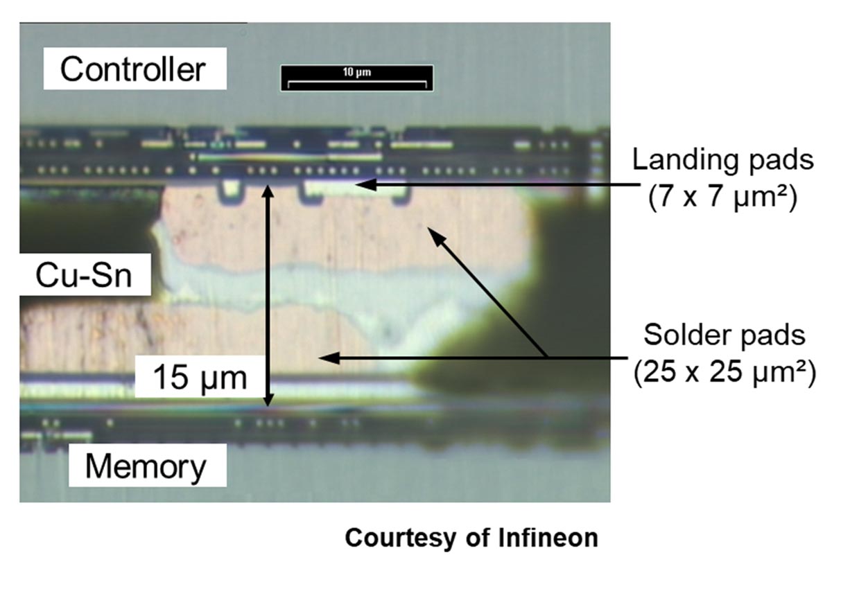
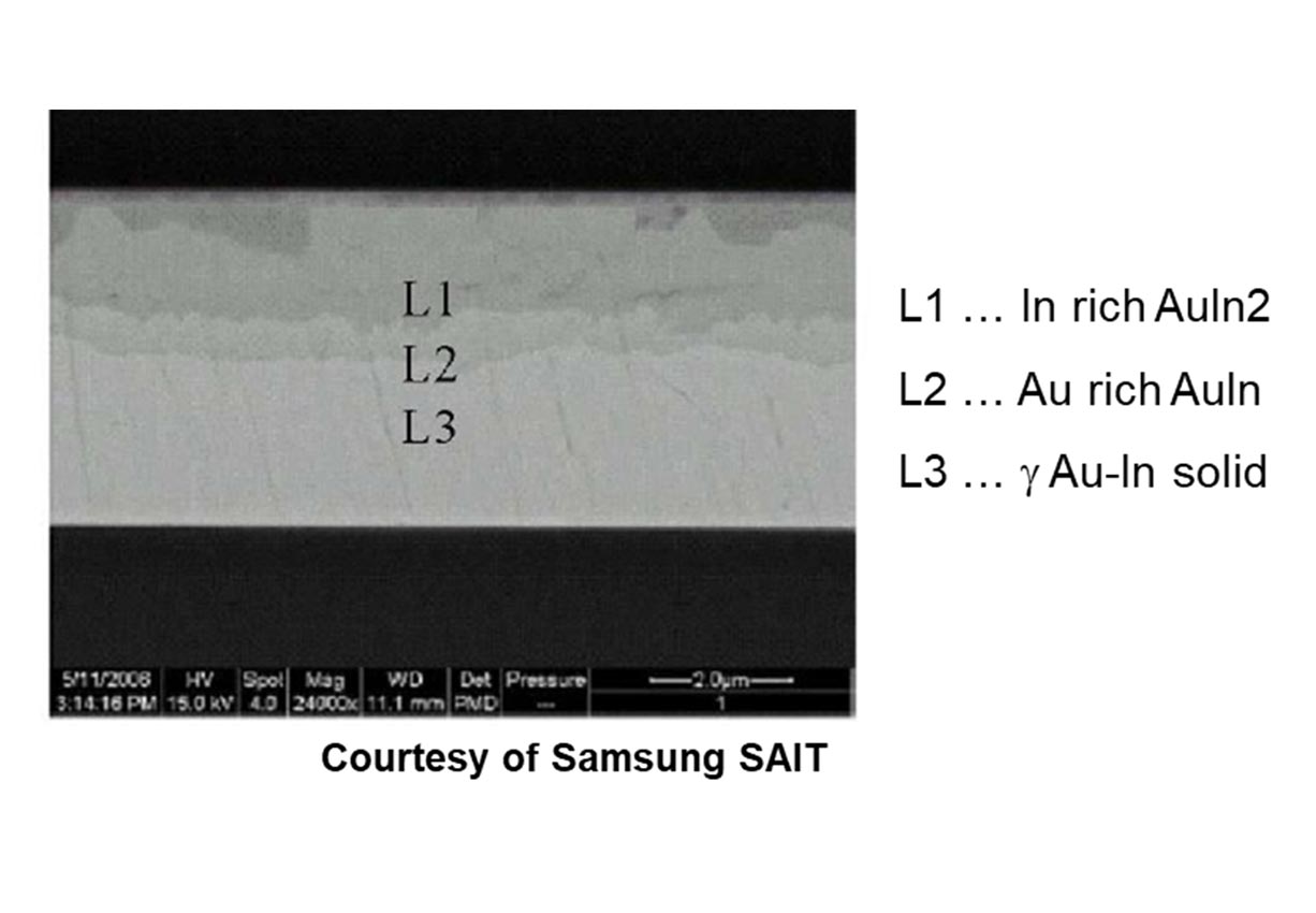
Transient Liquid Phase (TLP) bonding is often used when high-reliability bond lines or electric connections are needed. In this process, the interlayer melts, and the interlayer element diffuses into the substrate materials, thereby causing isothermal solidification. This results in a bond that has a higher melting point than the bonding temperature.
The unique characteristic feature of Transient liquid phase (TLP) bonding is that the liquid bond interface solidifies by diffusion but not by cooling below a melting point compared to eutectic bonding. This enables low process temperatures while providing much higher remelt temperature after joining the wafers. In particular, the interlayer is a low melting point material that moves into the lattice and grain boundaries of the high melting point parent materials, thereby forming an inter-metallic layer. In TLP, it is important to select a suitable interlayer based on the flow characteristics, stability and wettability in order to form a composition that provides faster diffusion characteristics and high reliability. Compared to other bonding technologies, TLP is an advanced type of solder bonding method that can form hermetic sealing at lower temperatures. It is ideal for MEMS vacuum packaging, as the process can be performed at low temperatures compatible with CMOS standards and the resulting bonded devices can withstand harsh environments with high temperatures.
Features
- Vacuum encapsulation
- Defined pressure encapsulation
- Conductive process
- Hermetic sealing
- Good mechanical strength
- Low temperature process
- Less applied force during bonding
- Very good post-bond alignment
- Applied in many metallic and ceramic systems
- Joints with uniform composition profile

Kontaktieren Sie unsere EVG-Technologieexperten!
Fragen?
Events

ICEP-HBS 2026
Hören Sie sich unsere Vorträge an:
“Hybrid Bonding and Interconnect Scaling: Driving Application Performance, Power and Cost by Mixing and Matching Semiconductor Technologies” von Representative Director Hiroshi Yamamoto.
“A predictive model for bond strengthening based on ion characteristics and the interface evolution in plasma activated fusion and hybrid bonding” von Deputy Team Leader Process Technology David Doppelbauer.
“From Scaling to Stacking: How Fusion and Hybrid Bonding enable Next-Generation High Performance Chip Architectures” von Business Development Manager Thomas Pleschke.
Für mehr Informationen klicken Sie hier.

Merck "The Future of Photonics — Materials Matter"
Hören Sie sich unseren Vortrag, gehalten von Business Development Manager Andrea Kronawitter, an: “Enabling Scalable Photonic Packaging using Nanoimprint Lithography”.
Nähere Informationen finden Sie hier.

CS / PIC / PE International Konferenz 2026
Besuchen Sie unseren Stand auf der CS / PIC and PE International Conference und hören Sie sich unsere Vorträge an:
"High performance GaN power devices enabled by wafer bonding" gehalten von Business Development Manager Elisabeth Brandl auf der CS Conference.
"Advancing Photonic Packaging and Integration Through UV Nanoimprint Lithography" gehalten von Senior Process Technology Engineer Patrick Schuster auf der PIC Conference.
- IR LayerRelease™ Technology
- MLE™ - Maskless Exposure Technologie
- Nanopräge-Lithographie (NIL) - SmartNIL®
- Wafer-Level Optics
- Optische Lithographie
- Fotolackverarbeitung
- Temporäres Bonden und De-Bonden
- Eutektisches Bonden
- Transient Liquid Phase (TLP) Bonden
- Anodisches Bonden
- Metall-Diffusionsbonden
- Hybrid- und Fusionsbonden
- Die-to-Wafer Fusion and Hybrid Bonding
- ComBond® Technologie
- Metrologie
Fragen zu unseren Technologien?
Kontaktieren Sie die EVG-Experten

