- Produkte
-
Technologien
- IR LayerRelease™ Technology
- MLE™ - Maskless Exposure Technologie
- Nanopräge-Lithographie (NIL) - SmartNIL®
- Wafer-Level Optics
- Optische Lithographie
- Fotolackverarbeitung
- Temporäres Bonden und De-Bonden
- Eutektisches Bonden
- Transient Liquid Phase (TLP) Bonden
- Anodisches Bonden
- Metall-Diffusionsbonden
- Hybrid- und Fusionsbonden
- Die-to-Wafer Fusion and Hybrid Bonding
- ComBond® Technologie
- Metrologie
- Unternehmen
- Karriere
Eutectic Bonding
Eutectic wafer bonding for reliable hermetic sealing
Introduction
Eutectic bonding, also called eutectic soldering, is where the combination of two or more metals allow direct transformation from solid to liquid state or vice versa at specific temperature without passing two-phase equilibrium. The eutectic temperature is much lower than the melting temperature of the materials that are involved in the bonding process. Eutectic bonding is ideal for high-vacuum applications as this process has very low outgassing.
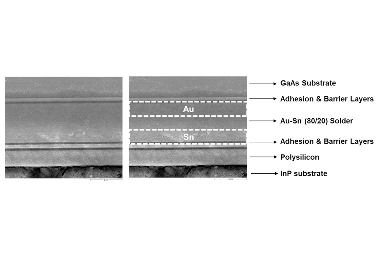
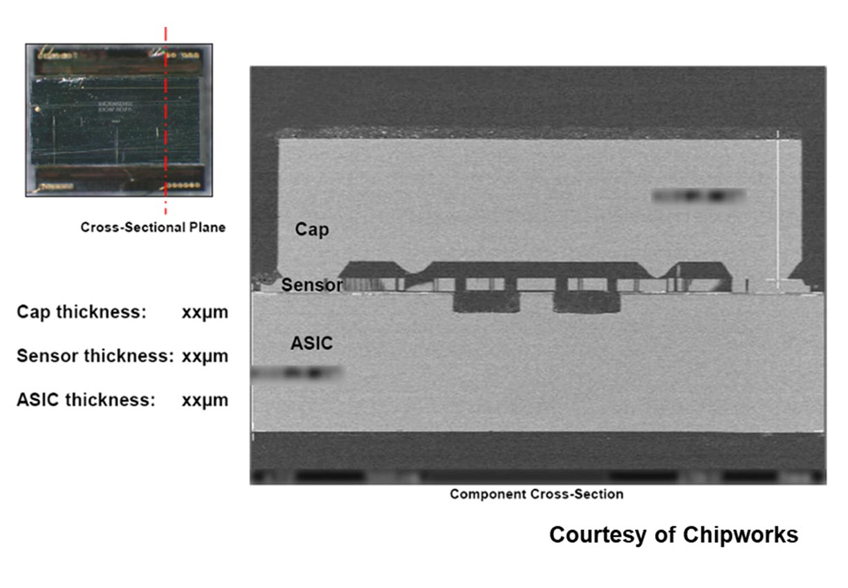
Eutectic wafer bonding is widely used in the MEMS industry for hermetic sealing, pressure or vacuum encapsulation as it allows highly reliable wafer-level processing for devices with the smallest form factors. The most common metals/alloys that are used in eutectic bonding are Al-Ge, Au-Sn and Au-In. However, there are many other material combinations available that can produce a eutectic bonding system. Additionally, the ability of silicon to alloy with metals like Au can also be the basis for eutectic bonding. All eutectic bonds must go through a liquid phase and thus are less sensitive to surface flatness irregularities, scratches and particles, thereby facilitating high volume manufacturing. Bonding temperature, time and pressure are the most important parameters for eutectic bonding where high bond strength can be achieved with low processing temperature and minimum resultant stress. Eutectic bonding can additionally enable hermetic sealing and electrical interconnections in a single process. Compared to other intermediate layers, such as adhesives or glass-frit, eutectic bonding also promotes better out-gassing and hermeticity.
Features
- Vacuum encapsulation
- Defined pressure encapsulation
- Conductive interface
- Hermetic sealing
- Good mechanical strength
- Narrow bond lines
- Good post-alignment bonding
- Low applied force
- Reversible process
- High fabrication yield

Kontaktieren Sie unsere EVG-Technologieexperten!
Fragen?
Events

ICEP 2025
Listen to our talks "Wafer Bonding Advances & 3D Applications" held by our Representative Director Hiroshi Yamamoto on 9:30 Wednesday, April 16 / Room B and "Hybrid Bonding for Heterogenous Integration" held by our Process Technology Manager Europe Gerald Mittendorfer on 12:40 Friday, April 18 / Room A.

JFS Conference and Compoundsemiconductor Industry Expo 2025
Besuchen Sie unseren Stand #A308

MicroNanoFabrication Annual Review Meeting 2025
Besuchen Sie unseren Stand auf dem MicroNanoFabrication Annual Review Meeting 2025!
- IR LayerRelease™ Technology
- MLE™ - Maskless Exposure Technologie
- Nanopräge-Lithographie (NIL) - SmartNIL®
- Wafer-Level Optics
- Optische Lithographie
- Fotolackverarbeitung
- Temporäres Bonden und De-Bonden
- Eutektisches Bonden
- Transient Liquid Phase (TLP) Bonden
- Anodisches Bonden
- Metall-Diffusionsbonden
- Hybrid- und Fusionsbonden
- Die-to-Wafer Fusion and Hybrid Bonding
- ComBond® Technologie
- Metrologie
Fragen zu unseren Technologien?
Kontaktieren Sie die EVG-Experten

