ZH
中文 (ZH)
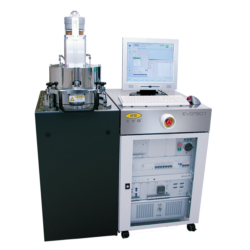
EVG®501
Wafer Bonding System
Versatile manual wafer bonding system for academia and industrial research
The EVG501 is a highly flexible wafer bonding system and supports all common wafer bonding processes such as anodic, glass frit, solder, eutectic, transient liquid phase, and direct. The easy access bond chamber and tooling design allows for quick and easy retooling for different wafer sizes and processes. This versatility is ideal for universities, R&D facilities, or low-volume production. The design of the bond chambers is similar to the EVG high-volume-manufacturing tools, such as the EVG GEMINI, and the bonding recipes are easily transferable, allowing for easy scale up of production volumes.
Features
- Unique pressure and temperature uniformity
- Compatible with EVG mechanical and optical aligners
- Flexible design and configurations for research
- From single chips to wafers
- Various processes (eutectic, solder, TLP, direct bonding)
- Optional turbopump (<1E-5mbar)
- Upgradeable for anodic bonding
- Open chamber design for easy conversion and maintenance
- Pilot production compatible
- Open chamber design for easy conversion and maintenance
- Smallest footprint for a 200 mm bonding system: 0.8 m2
- Recipes are fully compatible with EVG’s high-volume-manufacturing bonding systems
Technical Data
| Max contact force |
|---|
| 20 kN |
| Heater size | 150 mm | 200 mm |
|---|---|---|
| Minimum substrate dimension | single chips | 100 mm |
| Vacuum |
|---|
| Standard: 0.1 mbar |
| Optional: 1E-5 mbar |
| Max. temperature |
|---|
| 450 °C |
| Single chips processing |
|---|
| Yes |
| Bond chuck system / Alignment system |
|---|
| 150 mm heater: EVG®610, EVG®620, EVG®6200 |
| 200 mm heater: EVG®6200, SmartView® NT |
| Active water cooling |
|---|
| For bottom side |
| Power supply for anodic bonding |
|---|
| Max. voltage: 2 kV |
| Max. current: 50 mA |
| Loading chamber |
|---|
| Manual |

Talk to our EVG product experts!
Questions?
Questions about our products and technologies?
Contact the EVG experts
相关新闻
EV Group, Vietnam’s Authority of Information Technology Industry and PTIT Sign Memorandum of Understanding to Advance Vietnam's Semiconductor Capabilities
Mar, 2025
EV集团推出面向300毫米晶圆的下一代GEMINI®全自动生产晶圆键合系统,推动MEMS制造升级
Mar, 2025
EV Group Highlights Revolutionary Temporary Wafer Bonding and Debonding Solution for HBM and 3D DRAM at SEMICON Korea
Feb, 2025
