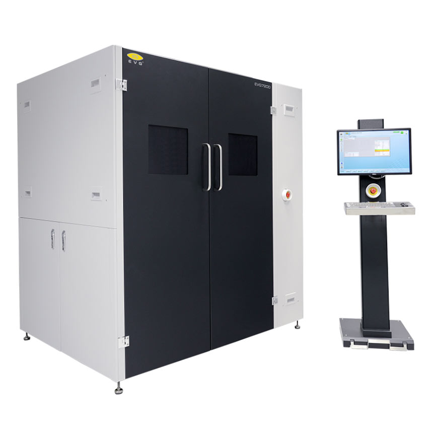
EVG®7200 LA
Large-Area SmartNIL® UV Nanoimprint Lithography System
UV Nanoimprint Lithography system for large area panels
The EVG7200 Large-Area UV Nanoimprint System scales nanoimprint lithography (NIL) to panel-size (Gen) substrates and is equipped with the latest evolution of SmartNIL technology. For applications such as displays, wire grid polarizers, biotechnology and photonic elements, which cannot be reduced in size, it is crucial to increase substrate utilization efficiency by increasing the pattern area. NIL has proven to be the most cost-efficient way to enable fabrication of nanopatterns on large areas as it is not limited by optical systems and can provide the best pattern fidelity for the smallest structures.
SmartNIL provides superior conformal imprint results down to 40 nm* utilizing a very robust and controllable tooling process. With unique and proven equipment capabilities, including unmatched ease of use, in conjunction with a high level of process expertise, EVG fulfills industry needs by driving nanoimprinting to the next level.
*resolution dependent on process and template
Features
- Proprietary SmartNIL® technology providing unmatched conformal imprinting over large areas
- Superior replication fidelity and uniformity
- Multiple-use polymer working stamp technology for longest master lifetime and significant cost savings
- Robust and precisely controllable processing
- Compatible with all commercially available imprint materials
- Available in R&D and high-volume manufacturing configuration
Technical Data
| Wafer diameter (substrate size) |
|---|
| 200 mm in diameter up to Gen3 (550 x 650 mm) |
| Resolution |
|---|
| 40 nm - 10 µm (resolution dependent upon template and process) |
| Supported Process |
|---|
| SmartNIL® |
| Exposure source |
|---|
| High-power narrow band (> 400 mW / cm²) |
| Alignment |
|---|
| Optional optical alignment: ≤ ± 15 µm |
| Automated separation |
|---|
| Supported |
| Mini environment and climate control |
|---|
| Optional |
| Working stamp fabrication |
|---|
| Supported |

Talk to our EVG product experts!
Questions?
Related technologies
Questions about our products and technologies?
Contact the EVG experts
