共晶接合
Eutectic wafer bonding for reliable hermetic sealing
Introduction
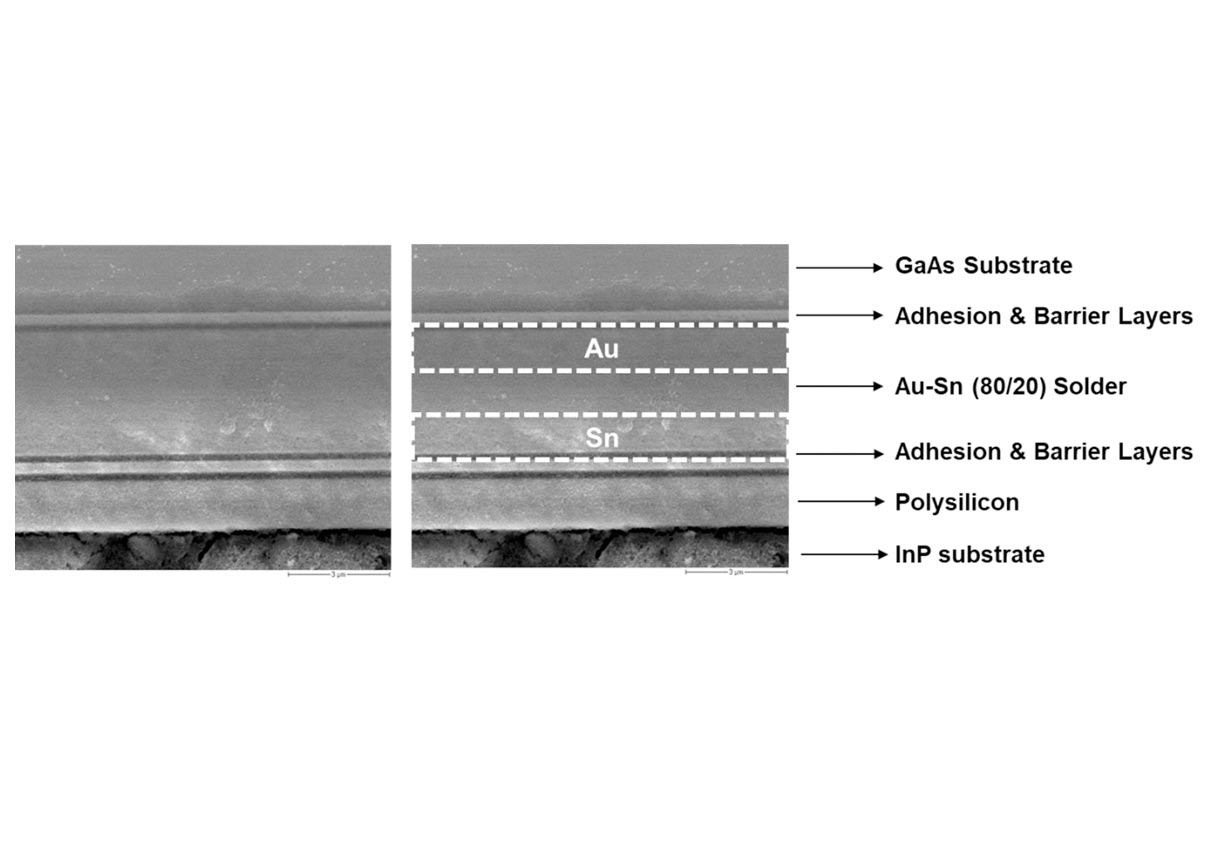
Eutectic bonding, also called eutectic soldering, is where the combination of two or more metals allow direct transformation from solid to liquid state or vice versa at specific temperature without passing two-phase equilibrium. The eutectic temperature is much lower than the melting temperature of the materials that are involved in the bonding process. Eutectic bonding is ideal for high-vacuum applications as this process has very low outgassing.
Eutectic wafer bonding is widely used in the MEMS industry for hermetic sealing, pressure or vacuum encapsulation as it allows highly reliable wafer-level processing for devices with the smallest form factors. The most common metals/alloys that are used in eutectic bonding are Al-Ge, Au-Sn and Au-In. However, there are many other material combinations available that can produce a eutectic bonding system. Additionally, the ability of silicon to alloy with metals like Au can also be the basis for eutectic bonding. All eutectic bonds must go through a liquid phase and thus are less sensitive to surface flatness irregularities, scratches and particles, thereby facilitating high volume manufacturing. Bonding temperature, time and pressure are the most important parameters for eutectic bonding where high bond strength can be achieved with low processing temperature and minimum resultant stress. Eutectic bonding can additionally enable hermetic sealing and electrical interconnections in a single process. Compared to other intermediate layers, such as adhesives or glass-frit, eutectic bonding also promotes better out-gassing and hermeticity.
Features
- Vacuum encapsulation
- Defined pressure encapsulation
- Conductive interface
- Hermetic sealing
- Good mechanical strength
- Narrow bond lines
- Good post-alignment bonding
- Low applied force
- Reversible process
- High fabrication yield

Talk to our EVG technology experts!
Questions?
Events

ICMAT 2025
Listen to our talk “Enhancing Nano-Imprinting Lithography: Synchronizing Process and Materials” held by Product Manager Dr. Anna Dudus.

ICEPT 2025
Listen to our presentation "Hybrid Bonding as Crucial Technology for Future Applications" held by Technology Development Manager Dr. Viorel Dragoi on 06th of August.
Semicon India 2025
Visit our booth 1520!
Questions about our technologies?
Contact the EVG experts

