- Products
-
Technologies
- IR LayerRelease™ Technology
- MLE™ - Maskless Exposure Technology
- Nanoimprint Lithography (NIL) - SmartNIL®
- Wafer Level Optics
- Optical Lithography
- Resist Processing Technology
- Temporary Bonding and Debonding
- Eutectic Bonding
- Transient Liquid Phase (TLP) Bonding
- Anodic Bonding
- Metal Diffusion Bonding
- Hybrid and Fusion Bonding
- Die-to-Wafer Fusion and Hybrid Bonding
- ComBond® Technology
- Metrology
- Company
- Careers
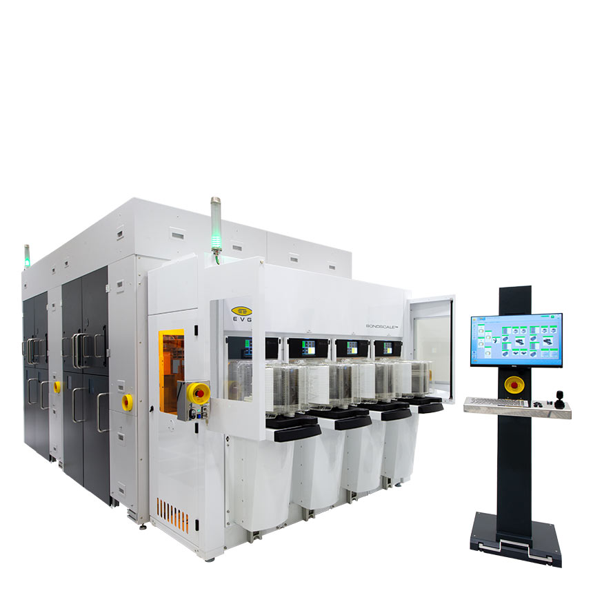
BONDSCALE®
Automated Production Fusion Bonding System
Enabling 3D Integration for More Moore
EVG BONDSCALE is designed to fulfill a wide range of fusion/molecular wafer bonding applications, including engineered substrate manufacturing and 3D integration approaches that use layer-transfer processing, such as monolithic 3D (M3D). With BONDSCALE, EVG is bringing wafer bonding to front-end semiconductor processing and helping to address long-term challenges for "More Moore" logic device scaling identified in the International Roadmap for Devices and Systems (IRDS). Incorporating an enhanced edge alignment technology, BONDSCALE provides a significant boost in wafer bond productivity and lower cost of ownership (CoO) compared to existing fusion bonding platforms.
BONDSCALE is being sold alongside EVG's industry benchmark GEMINI FB XT automated fusion bonding system, with each platform targeting different applications. While BONDSCALE will primarily focus on engineered substrate bonding and layer-transfer processing, the GEMINI FB XT will support applications requiring higher alignment accuracies, such as memory stacking, 3D systems on chip (SoC), backside illuminated CMOS image sensor stacking, and die partitioning.
Features
- Fully automated fusion/molecular wafer bonding applications on 200 mm and 300 mm substrates in a single platform
- Direct wafer bonding with plasma activation for heterogeneous integration of different materials, high-quality engineered substrates as well as thin-silicon layer-transfer applications
- Layer-transfer processes and engineered substrates enabling logic scaling, 3D integration such as M3, 3D VLSI including backside power distribution, N&P stacking, logic-on-memory, clustered functional stacks and beyond-CMOS adoption
Technical Data
| Wafer diameter (substrate size) |
|---|
| 200, 300 mm |
| Max. number or process modules |
|---|
| 8 |
| Throughput |
|---|
| Up to 40 wafers per hour |
| Handling system |
|---|
| 4 loadports |
| Features |
|---|
| Up to eight pre-processing modules like clean module, LowTemp™ plasma activation module, alignment verification module and debond module available |
| XT Frame concept for highest throughput with EFEM (Equipment Frontend Module) |
| Optical edge alignment module: Xmax/Ymax = 18 µm 3 σ |
Related downloads

Talk to our EVG product experts!
Questions?
Related technologies
Questions about our products and technologies?
Contact the EVG experts
