EN
English (EN)
Menu
- Products
-
Technologies
- IR LayerRelease™ Technology
- MLE™ - Maskless Exposure Technology
- Nanoimprint Lithography (NIL) - SmartNIL®
- Wafer Level Optics
- Optical Lithography
- Resist Processing Technology
- Temporary Bonding and Debonding
- Eutectic Bonding
- Transient Liquid Phase (TLP) Bonding
- Anodic Bonding
- Metal Diffusion Bonding
- Hybrid and Fusion Bonding
- Die-to-Wafer Fusion and Hybrid Bonding
- ComBond® Technology
- Metrology
- Company
- Careers
Search
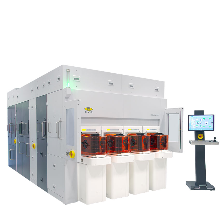
GEMINI® FB
Automated Production Wafer Bonding System
Integrated platform for high precision alignment and fusion bonding
Vertical stacking of semiconductor devices has become an increasingly viable approach to enabling continuous improvements in device density and performance. Wafer-to-wafer bonding is an essential process step to enable 3D stacked devices. EVG's GEMINI FB XT integrated fusion bonding system extends current standards and combines higher productivity with improved alignment and overlay accuracy for applications such as memory stacking, 3D systems on chip (SoC), backside illuminated CMOS image sensor stacking, and die partitioning. The system features the SmartView bond aligner, developed specifically for fusion and hybrid wafer bonding alignment requirements.
Features
- New SmartView® NT3 face-to-face bond aligner with sub 50 nm wafer-to-wafer alignment accuracy
- Up to six pre-processing modules like:
- Clean module
- LowTemp™ plasma activation module
- Alignment verification module
- Debond module
- XT Frame concept for highest throughput with EFEM (Equipment Frontend Module)
- Optional features:
- Debond module
- Thermocompression bond module
Technical Data
| Wafer diameter (substrate size) |
|---|
| 200, 300 mm |
| Max. number of process modules |
|---|
| 6 + SmartView® NT |
| Optional features |
|---|
| Debond module |
| Thermocompression bond module |
Related downloads

Talk to our EVG product experts!
Questions?
Related technologies
Questions about our products and technologies?
Contact the EVG experts
Related News
EV Group, Vietnam’s Authority of Information Technology Industry and PTIT Sign Memorandum of Understanding to Advance Vietnam's Semiconductor Capabilities
Mar, 2025
EV Group Advances 300-mm MEMS Manufacturing with Next-Generation GEMINI® Automated Production Wafer Bonding System
Mar, 2025
EV Group Highlights Revolutionary Temporary Wafer Bonding and Debonding Solution for HBM and 3D DRAM at SEMICON Korea
Feb, 2025
