JA
日本語 (JA)
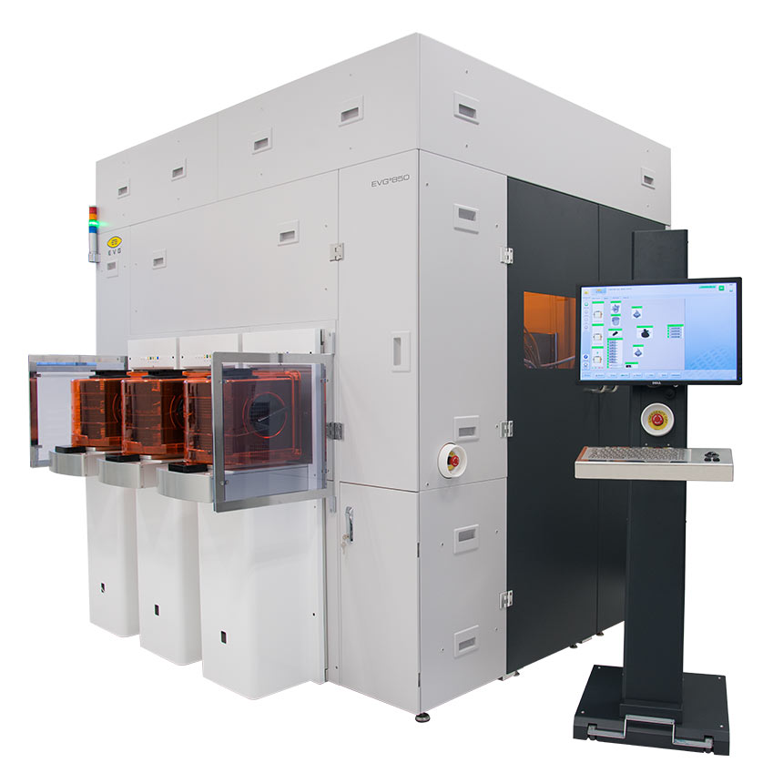
EVG®850
Automated Production Bonding System for SOI
Automated production bonding system for a wide range of fusion/molecular wafer bonding applications
SOI wafers are a promising new basic material for the microelectronics industry to produce faster and higher-performance microelectronic devices. Wafer bonding, as one key enabling technology for the SOI wafer fabrication process, achieves high-quality single-crystal silicon films on insulating substrates. With the EVG850 SOI production bonding system, all essential steps for SOI bonding – from cleaning to pre-bonding and IR-inspection – are combined. Thus, the EVG850 assures a high-yield production process for void-free SOI wafers. Being the only production system built to operate in high-throughput, high-yield environments, the EVG850 has been established as the industry standard in the SOI wafer market.
Features
- Production system built to operate in high-throughput, high-yield environments
- Automated cassette-to-cassette or FOUP-to-FOUP operation
- Contamination-free backside handling
- Megasonic and/or brush cleaning
- Pre-bonding with mechanical flat or notch alignment
- Advanced remote diagnostics
Technical Data
| Wafer diameter (substrate size) |
|---|
| 100 - 200, 150 - 300 mm |
| Fully-automated cassette-to-cassette operation |
| Pre-bonding chamber |
|---|
| Alignment type: flat-to-flat or notch-to-notch |
| Alignment accuracy: X and Y: ± 50 µm, Theta: ± 0.1 ° |
| Bond force: up to 5 N |
| Bond wave initiation position: flexible from wafer edge to center |
| Vacuum system: 9x10⁻² mbar (standard) and 9x10⁻³ mbar (option with turbo pump) |
| Cleaning station |
|---|
| Cleaning Method: rinse (standard), megasonic nozzle, megasonic area transducer, jet nozzle, brush (optional) |
| Chamber: made of PP or PFA (option) |
| Cleaning media: DI-water (standard), NH4OH and H2O2 with max. 2 % concentration (option) |
| Spinner chuck: vacuum chuck (standard) and edge handling chuck (option) made of metal ion free and clean materials |
| Rotation: up to 3000 rpm (in 5 s) |
| Cleaning arm: for up to 5 media lines (1 megasonic system uses 2 lines) |
| Optional features |
|---|
| ISO 3 mini-environment (according to ISO 14644) |
| LowTemp™ plasma activation chamber |
| IR-inspection station |

Talk to our EVG product experts!
Questions?
Related technologies
Questions about our products and technologies?
Contact the EVG experts
Related News
EV Group, Vietnam’s Authority of Information Technology Industry and PTIT Sign Memorandum of Understanding to Advance Vietnam's Semiconductor Capabilities
Mar, 2025
EV GROUP、次世代GEMINI®全自動量産用ウェーハ接合装置を発表 300mm MEMS製造の進化に貢献
Mar, 2025
EV Group、HBMおよび3D DRAM向けの画期的なウェーハ仮接合と剝離ソリューションを SEMICON Koreaで発表
Feb, 2025
